Sony wants TSMC's help to make image sensors
Published: (May 8, 2026 at 07:35 AM EDT)
2 min read
Source: Engadget
Source: Engadget
Sony‑TSMC Joint Venture Overview
Sony is teaming up with chip giant TSMC on a new joint venture in Japan to build the next generation of image sensors. The partnership will be led by Sony and based at its newly‑built facility in Koshi City, while leveraging TSMC’s “strengths in process technology and manufacturing excellence.” Both companies are also seeking support from the Japanese government for additional financial incentives.
Strategic Context
Shift Toward an “Fab‑Light” Model
- CEO Hiroki Totoki frames the move as the “first step to becoming fab‑light,” aiming to reduce Sony’s in‑house manufacturing footprint.
- This follows Sony’s earlier decision to exit TV manufacturing, handing control of its Bravia division to TCL.
Need for Advanced Process Capabilities
- Stacking technology is making image sensors increasingly complex.
- Partnering with TSMC provides the manufacturing muscle Sony needs to stay competitive.
Potential Impact
If Sony and TSMC successfully combine their strengths, the joint venture could accelerate development of image sensors for:
- Smartphones (e.g., iPhone, Pixel, OnePlus)
- Cameras (e.g., Nikon, Fujifilm, Leica)
- Vehicles and other emerging applications
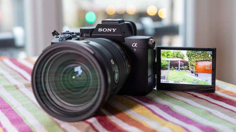
Sony currently supplies the gold‑standard imaging sensor used across these markets.
Risks and Considerations
- Competitors might bypass Sony entirely and work directly with TSMC for future sensor needs, potentially eroding Sony’s market share.
All URLs, code snippets, and technical terms have been retained exactly as in the original source.