Post-silicon era gets closer as industry giants crack the 2D transistor scaling bottleneck with breakthrough tech — imec, ASML, and TSMC fab complementary 2D-material transistors at 50nm pitch on a 300mm wafer
Source: Tom’s Hardware
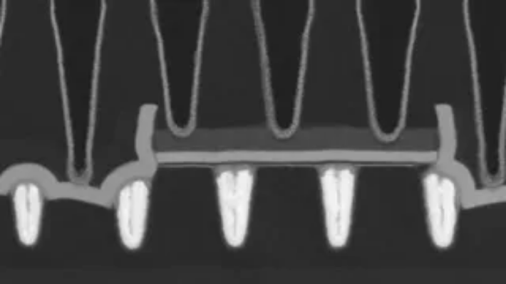
(Image credit: imec/ASML/TSMC)
Imec, ASML, and TSMC have integrated both n-type and p-type transistors with atomically thin 2D channels on a single 300mm wafer at a 50nm contacted poly pitch, the tightest pitch demonstrated to date for complementary 2D devices and one that lands within range of leading-edge silicon.
The trio presented the work this week at the IEEE/JSAP Symposium on VLSI Technology and Circuits, using a single EUV exposure to print channel lengths as short as 28nm. Imec reported that 94% of the integrated transistors switched correctly, with an on/off current ratio above 100,000. The n-channel devices use molybdenum disulfide (MoS2), while the p-channel devices use tungsten diselenide (WSe2) or tungsten disulfide (WS2).
Luke James is a freelance writer and journalist. Although his background is in legal, he has a personal interest in all things tech, especially hardware and microelectronics, and anything regulatory.